FP-21T Precision Introduction Example
Computer-aided modeling and design of printed-circuit
boards fabricated using MITS FP-21T Precision milling
machine
Professor Dr. Antonije Djordjevic
University of Belgrade
School of Electrical Engineering
Serbia
E-mail: edjordja@etf.rs
MITS FP-21T Precision milling machine produces microwave
circuits with high precision on both
soft and hard substrates. The high resolution of 50µm
makes this PCB prototyping machine
convenient for producing circuits that operate even in the
millimeter-wave region.
At the School of Electrical Engineering, University of Belgrade,
we have been investigating specific
approaches to the modeling and design of microwave printed
circuits that are produced by milling.
Two issues are considered: cross-section profiles of milled
transmission lines and production
optimization.
The shape of traces (lines) produced by the milling process
depends on the tool used. It is possible
to obtain vertical and sloped sides of the copper traces
(Figure 1). The milling tools remove not only
copper, but also slightly dig into the substrate, leaving
a grooved surface.
The performance of microwave circuits is affected by the
shape of the conductors and dielectrics.
For example, the characteristic impedance of the microstrip
line and the velocity of wave propagation
increase if the dielectric near the trace is grooved.
In order to accurately predict the circuit performance,we
have developed quasi-static models for
machined transmission lines, using the approach presented
in Reference [1], which are to be
compared with measurement results on PCBs produced using
our MITS FP-21T Precision
milling machine.


Figure 1. Typical profiles of machined PCB traces
(cross section). |
Rubbing out large inactive copper surfaces around microwave
microstrip circuits is usually required
in order to prevent deterioration of the circuit performance.
Large copper surfaces and the ground
plane create resonators that are coupled to the microwave
circuit, which can result in glitches in the
scattering parameters and create strong radiation.
On the other hand, milling large copper surfaces in the
rub-out process requires long processing time
and tool wear out.
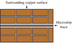
Using software WIPL-D [2], [3], we have developed computer
models that simulate large copper patches
in the vicinity of microstrip circuits (Figure 2). These
models are used to design slots in large copper
surfaces that push the parasitic resonances safely above
the operating frequency band of the microwave
circuit. In this way, large copper surfaces in the vicinity
of microstrip circuits are passivized with only a few
milled grooves, and the possibility of inadvertent influence
on the circuit performance is minimized.

Figure 2. Microstrip trace with passivized neighboring
copper surfaces (top view).
|
References
- A.R.Djordjevic, M.B. Bazdar, R.F. Harrington, T.K.
Sarkar, LINPAR for Windows:
Matrix Parameters for Multiconductor Transmission Lines,
Version 2.0, Software and
User's Manual, Artech House, Norwood, 1999.
- B.M. Kolundzija, J.S. Ognjanovic, T.K. Sarkar, D.S.
Sumic, M.M. Paramentic, B.B. Janic,
D.I. Olcan, D.V. Tosic, M.S. Tasic, WIPL-D Microwave
Software and User's Manual,
WIPL D/Artech House, Belgrade/Norwood, 2005.
- WIPL-D Pro v6.4, "Software and User's Manual," WIPL-D
d.o.o., Belgrade, 2008.
www.wipl-d.com
Read more>>
Using MITS FP-21T Precision
milling machine at the University of Belgrade
|
|
MITS
General Catalog

English
(PDF file / 1.8MB)
MITS Electronics
E-MAIL

Contact us : Inquiry Form
|

