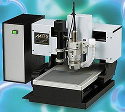
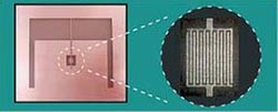
Prototyping Printed Board Making System For thin film patterning
|
|||||||||||||||||||||||||||||||||||||||||||||||||
|
Can we apply this for thin films on SrTiO3 substrates? Hall bar and so on... 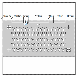
|
Difficulty No. 1
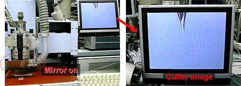
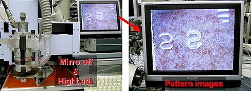
Detection of milling cutter contact with SrTiO3 substratePrinted board is conductive due to surface thick metal layer (up to 10 µm) and can be detected by electric contact.
But SrTiO3 is insulator.
Even if conductive film is deposited, it is too thin for electric detection.
Image Detection
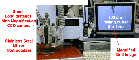
Milling of hard, fragile SrTiO3
Printed board is soft, which includes surface metal layer and plastic board
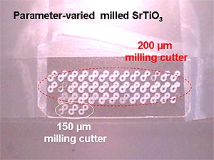
Milling parameters optimization
Parameters optimization summary
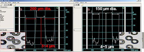
Parameters optimization summary
Superiority of FP-21T Precision
- As the procedure of solid-state science -
Even if conductive film is deposited, it is too thin for electric detection.
Image Detection

Difficulty No. 2
Milling of hard, fragile SrTiO3Printed board is soft, which includes surface metal layer and plastic board
Milling parameters optimization
Milling parameters
etc.
|
 |
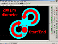
|
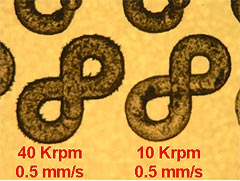 Higer rotation speed does not necessarily lead to the fine finishes. |
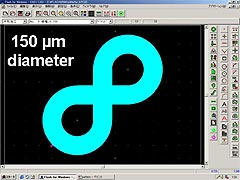
|
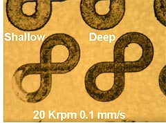 |
Parameters optimization summary
| - | Lower rotation speed is better Although too low speed is unstable to hold constant speed |
Opt.: 20 Krpm |
| - | Depth is not so critical Although too deep results in shorter cutter life time |
Opt.: up to 5 µm |
| - | Lower lateral milling speed is better | Min.: 0.1 mm/s |
| - | Milling cutter diameter dependence is unknown | Hopefully no dependence |

Parameters optimization summary


Superiority of FP-21T Precision
- As the procedure of solid-state science -
- You are able to process easily and dry
- You can omit the photo lithographic process (No need to buy expensive machines)
- You can process it without chemical reagent
- You can process the oxidative product
- You can easily produce Hall bar
- Very precise and accurate
Read more>>The relationship among the spindle rotating speed, processing speed, and the tools
MITS General Catalog
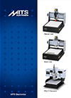
English
(PDF file / 1.8MB)
MITS Electronics
Contact us : Inquiry Form