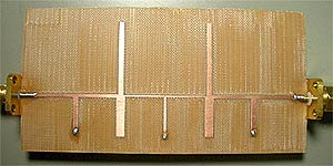
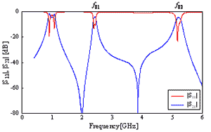
Let us illustrate the procedure of PCB processing beginning from the pattern-designing to the data evaluation, by taking the case of the high-frequency filter (dual-band filter with micro-strip line) as an example |
||||||||||||||||||||||||||||||||||||||||
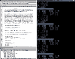
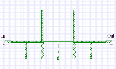
| At the preliminary step towards designing the print circuit pattern by PCB processing machine, we calculate the structural parameter of the filter by the computer program, and evaluate the characteristics of the electric transmission. |
|
|
|
||
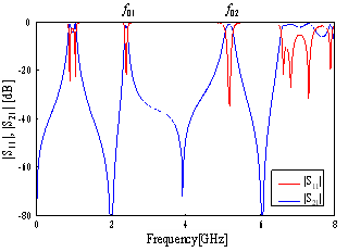
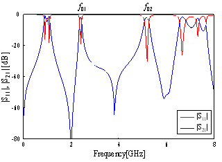
| This figure shows the outcome of the calculated electric transmission characteristics by the circuit simulator in the light of the result of designing the dual-band-filter using the microstrip substrate. |
|
|
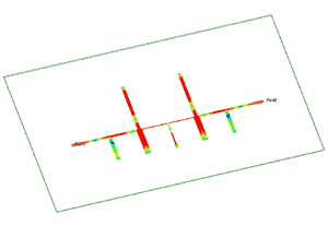
| We can also calculate the distribution of the electric current density, as well as the characteristics of the electric transmission, by analyzing the pattern shape of trial circuit using structural simulators such as the electromagnetic field simulator. |
|
||
| |
|||
| We are able to grasp and visualize the
electromagnetic distribution by the structural simulator.
Also, we can make use of that data for the designing
of the circuit board. (This circuit is analyzed by Ansoft Designer Ver.3.0 by courtesy of Ansoft Japan) |
|
||

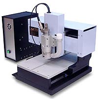
Based on the data acquired by the result of the designing, simulation, and by the analysis,
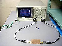
we produce the circuit board using the PCB processing machine. Next, we estimate the
circuit board that we produced and evaluate the characteristics of them by comparing
the result of the simulation and analysis.
|
|
||
|
|
(The designing and measuring of the above circuit are performed by the collaboration
with TAIYO YUDEN CO.,LTD.)
50µm(2mil) line and space, the state of the art!
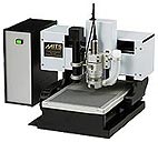
FP-21T Precision
Stepping method and non-contacting pressure foot lead to the fine processing technology
For RF board making to processing various materials! FP-21T
MITS General Catalog

English
(PDF file / 1.8MB)
MITS Electronics
Contact us : Inquiry Form


