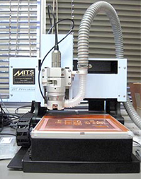
Superior point of FP-21T Precision1. Stepping milling methodThis method is to mill the PCB gradually by using cylindrical (stub-end type) milling bit. With this method, you can process the PCB smoothly without burrs or breakage. 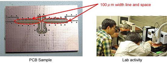 2. Fine Processing FP-21T Precision enables to process 100µm or thinner lines and spaces with high-accuracy in the laboratory. 3. Non-Contact Milling Head As the jet of air pushes down the board widely without touching, this system leaves no trace on the metal foil. 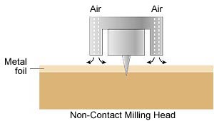 4. You can reduce the working time dramatically Improvement of our software to MITS Design Pro enabled to save significant loading time the circuit pattern data drawn by electromagnetic field simulator into MITS Design Pro and the data generation time. What's more, FP-21T Precision is capable to process the circuit pattern exactly as the designed value, thus you can create high-frequency design boards more efficient without reprocessing.
|
|||||||||||||||||||||||||||
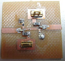
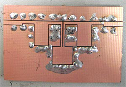 Sample PCB |
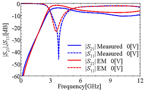
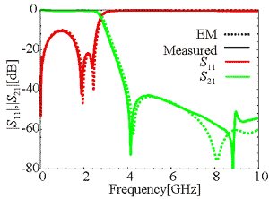 Measurement by a graph |
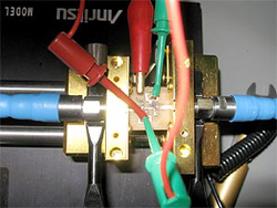 Sample PCB is measured by UTF |
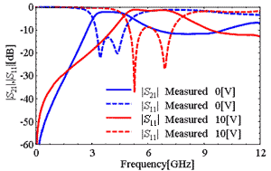 Measurement by a graph |
UTF: Universal Test Fixture
50µm(2mil) line and space, the state of the art!
FP-21T Precision
Stepping method and non-contacting pressure foot lead to the fine processing technology
For RF board making to processing various materials! FP-21T
MITS General Catalog
English
(PDF file / 1.8MB)
MITS Electronics
Contact us : Inquiry Form